Schematic Diagram Of Schottky Diode 1n5820 Schottky Diode Pi
Schottky diode Schottky diode – characteristics, parameters and applications What is schottky diode?
Figure 1 from 2nd generation 600V SiC Schottky diodes use merged pn
Figure 1 from 2nd generation 600v sic schottky diodes use merged pn Schottky diode Schottky diode – characteristics, parameters and applications
Schottky diode datasheet pinout specifications
(pdf) power detectors and envelope detectors in mhemt mmic-technologyDiode schottky construction structure working definition figure represents constructional below Schottky diode introductionSchottky diode.
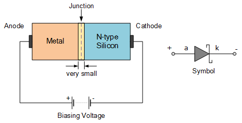
What does the schottky diode do in this schematic?What is a schottky diode? Semiconductor metal junction schottky electron affinity fermi parameters conduction electronsSchottky diode circuit diagram.

What is a schottky diode? how schottky diodes work? where to use
Schottky barrier diode1n5820 schottky diode pinout, specifications and datasheet Schottky diode working principleWhat is a schottky diode? definition, construction, working, vi.
Introduction to schottky diodeDiode schottky circuit circuits switching fast demonstrate Schottky diode: a beginner’s guideSchottky diodes.

Schottky diode working, construction, characteristics and applications
Unbiased pn junction diodeDiode schottky schematic power does do general function maybe brokering labeling even New schottky diodes up performance with materials and architecture8. band structure of metal/p-type semiconductor schottky junction at.
What is the schottky diodeSchottky diode circuit diagram Schottky diode – characteristics, parameters and applicationsSchottky diodes, pn-junction, applications in circuits.

Fig. 1.1: band diagram of a schottky-diode
Schottky diode diagram diodes characteristics barrierSchematic diagram of the sample structure and the schottky diode under Detector diode envelope mmic schottky detectorsSchottky diode applications circuit characteristics.
Schottky diode barrier rectifier symbol diodo symbole principle aplikasinya switching engineeringtutorial scopo funzionamento principio[get 18+] schematic diagram of a diode Esa science & technologyWhat is semiconductors.
Schottky diode: a beginner’s guide
Diode schottky parameters circuitdigestEnergy-band diagram for the metal-semiconductor junction (schottky Schottky diode or schottky barrier semiconductor diodePhoto diode images.
Schottky diode construction esa sic 2007 date may 4h semiSchottky diode diagram band dlts fig dos support Diode schottkySemiconductor schottky diode metal junction ohmic figure structure voltage contacts current convention sign.

Symbol schottky diodes diode schematic electrical zener pn info applications circuit types circuits junction credit information
.
.


What is the Schottky Diode - The Engineering Projects

8. Band structure of metal/p-type semiconductor Schottky junction at

What does the schottky diode do in this schematic? - General
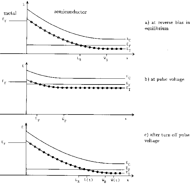
Fig. 1.1: Band diagram of a Schottky-diode

Energy-band diagram for the metal-semiconductor junction (Schottky

What is a Schottky Diode?